|
|
|
 |


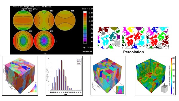
| X-Ray Diffraction | 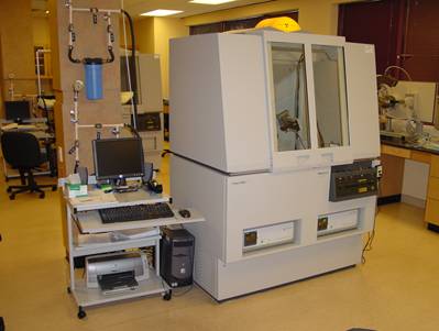 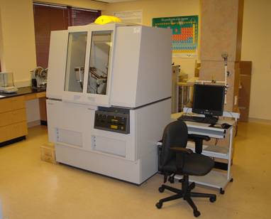 PANalytical X’Pert PRO Alpha-1, PANalytical X’Pert PRO MPD, PANalytical X’Pert PRO MPD X-ray Analysis Group at GATech |
| MoCVD and RESS Facility | 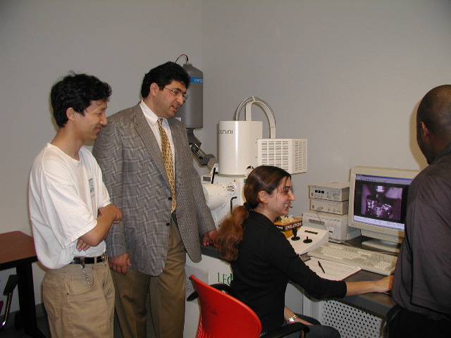 Metal-organic Chemical Vapor Deposition (MOCVD) and supercritical fluid extraction and the rapid expansion of supercritical fluid solutions (RESS), techniques were applied for the preparation of:
|
| Chemical Vapor Deposition for In-Field Processing | 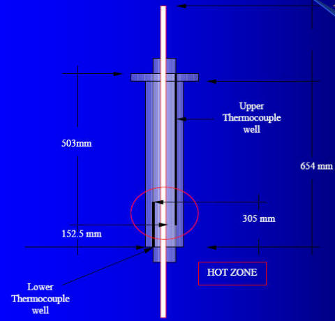 In-field & 0-field Processing (1200C) Thin film Nano-tubes |
| Prototype for Nano-Tube CVD Production | 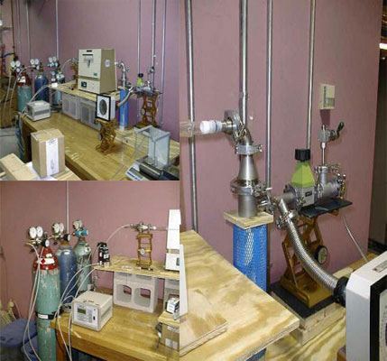 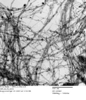 Scale bar: 500nm, HV: 200KV, TEM Mag: 50000X 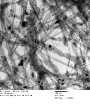 Scale bar: 100nm, HV: 200KV, TEM Mag: 150000X 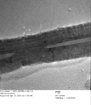 Scale bar: 5nm, HV: 200KV, TEM Mag: 1200000X |
| Magnetic Processing | 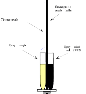 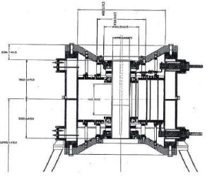
|
| Chemical Vapor Deposition | 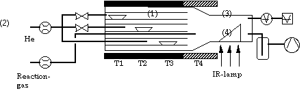 |
| CVD Reaction | 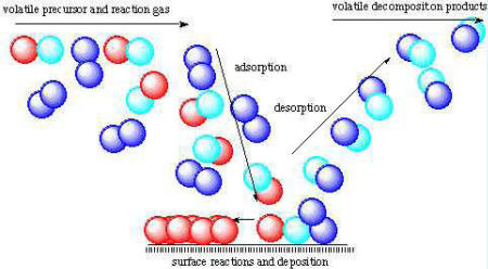 |
| System Assembled | 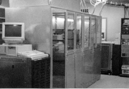 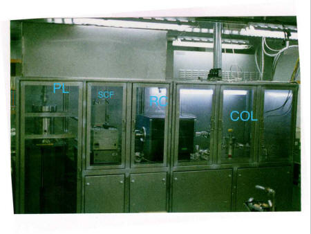 PL: Plasma chamber, SCF: super critical fluid, RC: reaction Chamber, COL: Collector |
| Micro-nanofabrication | Variety of Micro/nanofabrication facilities for physical and chemical deposition such as PECVD, Atomic Layer Deposition (ALD), etc. available at Georgia Tech Microelectronics Research Center (Institute for Electronics and Nanotechnology: http://cleanroom.ien.gatech.edu/ |
| Characterization | * Characterization facilities available at Georgia Tech Microelectronics Research Center (Institute for Electronics and Nanotechnology: http://cleanroom.ien.gatech.edu/ - Field-Emission Scanning Electron Microscopy (SEM/EDS) (Zeiss Ultra60 FE-SEM) - Focused Ion Beam (FIB) (FEI Quanta, FEI Nova) - Atomic Force Microscopy (AFM) * Georgia Tech Center for Nanostructure Characterization and Fabrication: http://cncf.nanoscience.gatech.edu/ - Transmission Electron Microscopy (JEOL 4000EX, JEOL 100 CX) |